Siemens Digital Industries Software moved to simplify the drafting and production of 2.5D and 3D integrated circuit (IC) designs typically used for high-bandwidth memory functions.
The company unveiled a pair of products to aid semiconductor designers, promoting the potential to lower risk, and boost design yield and efficiency in the drafting process.
Siemens’ Innovater3D IC product focuses on providing predictability in the “planning and heterogeneous integration”, along with the application of substrates and interposers.
The product employs AI to provide user experience benefits and is optimised for designs with 5 million or more pins.
Siemens explained Innovater3D IC offers a “consolidated cockpit” for building digital twins, elements covering substrate and interposer use, analysis tools covering chiplet-to-chiplet and die-to-die interface compliance, and data management systems.
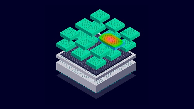
The company also introduced Calibre 3DStress to tackle variances in specifications between “designs validated and tested at the die level” once packaging takes place.
Siemens stated the product targets “accurate, transistor-level analysis, verification and debugging of thermo-mechanical stresses”, enabling chip designers to evaluate the impact of packaging “earlier in the development cycle”.
“Calibre 3DStress represents an important part of Siemens’ 3D IC multi-physics software portfolio”, along with being foundational to its “digital twin and semiconductor development workflows”, the company stated.